Hollow nano and micro bumps
Low-Temperature and Low-Pressure Bonding Technology
Overview
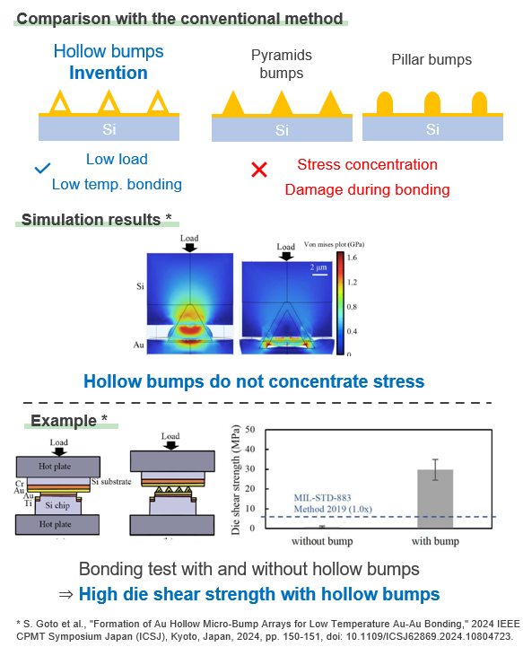
Bonding between components is a critical step in semiconductor packaging, especially as devices become more complex and sensitive. Traditional bump structures like pyramids or cones rely on stress concentration to achieve strong joints. However, this often results in damage to the device or substrate.
Our novel hollow bump technology addresses this issue by allowing the bump to deform plastically under low loads. This exposes fresh metal surfaces, low-temperature bonding with minimal stress. This approach reduces the risk of mechanical damage while maintaining strong interconnect performance, offering a promising solution for semiconductor assembly.
Features・Outstandings
Product Application
・Semiconductor and component mounting
・Module and component bonding
IP Data
IP No. : Not published
Inventor : HIGURASHI Eiji, TAKEUCHI Kai, GOTO Shintaro
keyword : mounting、packaging、low temperature、low pressure、bump